Electrical contact to molecules in semiconductor structures established for the first time
Electrical circuits are constantly being scaled down and extended with specific functions. A new method now allows electrical contact to be established with simple molecules on a conventional silicon chip. The technique promises to bring advances in sensor technology and medicine, as reported in the journal Nature by chemists from the University of Basel and researchers from IBM Research – Zurich in Rüschlikon.
12 July 2018
To further develop semiconductor technology, the field of molecular electronics is seeking to manufacture circuit components from individual molecules instead of silicon. Because of their unique electronic properties, molecules are suited to applications that cannot be implemented using conventional silicon technology. However, this requires reliable and inexpensive methods for creating electrical contacts at the two ends of a molecule.
The ability to produce thousands of elements
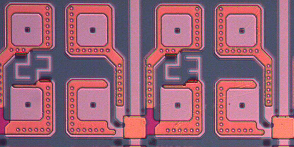
Researchers from the University of Basel and IBM Research – Zurich have now developed a technique that allows electrical contact to individual molecules to be established. Thousands of stable metal-molecule-metal components can be produced simultaneously by depositing a film of nanoparticles onto the molecules, without compromising the properties of the molecules. This approach was demonstrated using alkane-dithiol compounds, which are made up of carbon, hydrogen, and sulfur.
The researchers used a type of sandwich construction in which an interlayer of molecules is brought into contact with metallic electrodes from above and below. The lower electrode consists of a layer of platinum, which is coated with a layer of non-conducting material. Tiny pores are then etched into this layer to produce arbitrary patterns of compartments of different sizes, inside which there is an electrical contact with the platinum electrode.
Self-assembled monolayers
The researchers then took advantage of the ability of certain molecules to self-assemble. Onto the pattern of pores, they applied a solution containing alkane-dithiol molecules, which self-assemble into the pores, forminga densely packed monolayer film. Within this film, the individual molecules exhibit a regular arrangement and an electrical connection with the lower platinum electrode. Electrical contact with the molecular layer is established via an upper electrode made of gold nanoparticles.
The new technique largely resolves the issues that previously hampered the creation of electrical contacts to molecules – such as high contact resistance or short circuits by filaments penetrating the film. Building blocks fabricated by this method can be operated under standard conditions and provide long-term stability. Moreover, the method can be applied to a variety of other molecular systems and opens up new avenues for integrating molecular compounds into solid-state devices. Its applications could include new types of instruments in the fields of sensor technology and medicine.
“Our approach will help speed up the development of chemically fabricated and controllable electronic and sensor components,” says Professor Marcel Mayor of the Department of Chemistry at the University of Basel. The project received significant funding from the National Center of Competence in Research (NCCR) for Molecular Systems Engineering, in which the University of Basel and ETH Zurich are leading houses.
Original source
Gabriel Puebla-Hellmann, Koushik Venkatesan, Marcel Mayor, and Emanuel Lörtscher
Metallic nanoparticle contacts for high-yield, ambient-stable molecular-monolayer devices
Nature (2018), doi: 10.1038/s41586-018-0275-z
Further information
Professor Marcel Mayor, University of Basel, Department of Chemistry, Tel. +41 61 207 10 06, Email: marcel.mayor@unibas.ch