Energy flow in semiconductors: new insights thanks to ultrafast spectroscopy
For the first time and with unprecedented accuracy, a team of researchers from the University of Basel has observed unique energy flow mechanisms in a semiconductor material following excitation by extremely short laser pulses. Gaining a better understanding of these energy flow is vital for improving the efficiency of electronic devices and computer chips.
19 January 2026 | Christel Möller
Whether in a smartphone or laptop, semiconductors form the basis of modern electronics and accompany us constantly in everyday life. The processes taking place inside these materials are the subject of ongoing research. When the electrons in a semiconductor material are activated using light or an electrical voltage, the excited electrons also set the atomic lattice in motion. This results in collective vibrations of the atoms, known as phonons or lattice vibrations, which interact with each other and with the electrons themselves.
These tiny lattice vibrations play a vital role in how energy flows and dissipates through the material — in other words, in how efficiently the energy is redistributed and how strongly the material heats up. Different approaches can be used to control and monitor the propagation of lattice vibrations — and therefore to make the semiconductor more effective and more efficient.
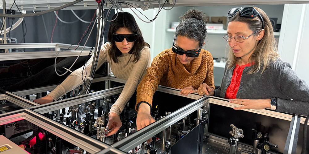
Detailed knowledge of the mechanisms of energy loss and potential overheating is essential in order to design new materials and devices that heat up less, recover faster or respond to external excitation more precisely. A team led by Professor Ilaria Zardo from the University of Basel reports on the unprecedented accuracy they achieved in measurements of energy flow processes within the semiconductor germanium, which is frequently used in computer technology, as published in the journal Advanced Science.
Energy flow following ultrafast excitation
The team from the Department of Physics and the Swiss Nanoscience Institute has specifically developed a unique technique that can be used to accurately measure how electrons and phonons move and exchange energy within the crystal lattice of the analyzed material following excitation with ultrashort laser pulses of just 30 femtoseconds (1 femtosecond is equal to 10-15 seconds). By doing so, the physicists were able to show how energy flows, how it is transferred and how it is converted into heat within the material.
“For the first time, a combination of two spectroscopic techniques allowed us to observe how energy is transferred step-by-step from the electronic system to the lattice. We can also observe how the frequency, intensity and duration of lattice vibrations change over time following excitation,” explains Dr. Grazia Raciti, first author of the publication.
Unimaginably small
Here, one of the spectroscopic techniques, known as time-resolved Raman spectroscopy, measures tiny changes in the vibrations of the atomic lattice. The second technique, known as transient reflection spectroscopy, records the change in light behavior following brief excitation.
-
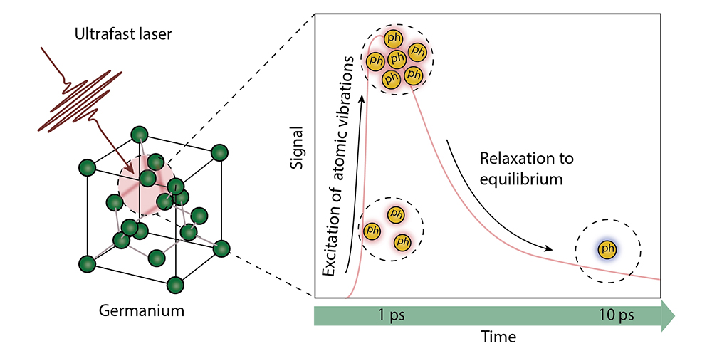 The semiconductor material germanium is excited using an ultrafast laser. With a pioneering combination of two methods, the researchers can then measure how the atomic lattice vibrations (phonons) “relax” in the picosecond range after excitation. (Illustration: G. Raciti; Department of Physics, University of Basel)link.zoom
The challenge in these measurements is related to the tiny signals and timescale on which the interactions take place. With measurements running for a period of 48 hours, the system is excited with a short laser pulse once per microsecond. The observed changes in the system then take place on the picosecond timescale. Dr. Begoña Abad Mayor, a researcher in Zardo’s team, explains these unimaginably small dimensions using an analogy: “If we imagine that the time gap between two laser pulses (which is actually 1 microsecond) lasts 10 days, then the sample’s response that we record in the semiconductor lasts just a second.”
Accordingly, these measurements access incredibly fast timescales with extremely high sensitivity. The researchers can detect tiny changes of less than 1 percent in intensity and less than 0.2 cm⁻¹ in frequency. With this atomic-scale time and energy resolution, it is possible to differentiate between various mechanisms of energy loss.
The researchers from the Department of Physics and the Swiss Nanoscience Institute of the University of Basel supplemented their experimental investigations with state-of-the-art computer simulations. This enabled them to understand in detail the physical processes underlying the measurement results.
Understanding needed for further development
The combined result provides a detailed picture of how energy is distributed and dissipated in germanium following ultrafast excitation. “This basic research is vital in order to understand and further develop modern electronics and novel phononic components and may therefore lead to better chips, sensors or other electronic devices,” says Zardo.
Original publication
Grazia Raciti et al.
Unraveling Energy Flow Mechanisms in Semiconductors by Ultrafast Spectroscopy: Germanium as a Case Study
Advanced Science (2026), doi: 10.1002/advs.202515470